- 您现在的位置:买卖IC网 > Sheet目录464 > IXTQ160N085T (IXYS)MOSFET N-CH 85V 160A TO-3P
�� �
�
�Advance� Technical� Information�
�Trench� Gate�
�Power� MOSFET�
�IXTQ� 160N085T�
�IXTA� 160N085T�
�IXTP� 160N085T�
�V� DSS�
�I� D25�
�R� DS(on)�
�=� 85� V�
�=� 160� A�
�=� 6.0� m� ?�
�N-Channel� Enhancement� Mode�
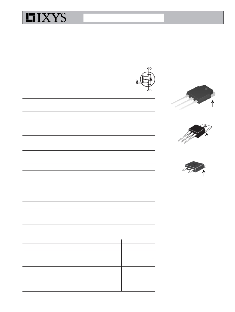
�TO-3P� (IXTQ)�
�Symbol�
�Test� Conditions�
�Maximum� Ratings�
�V� DSS�
�V� DGR�
�T� J� =� 25� °� C� to� 175� °� C�
�T� J� =� 25� °� C� to� 175� °� C;� R� GS� =� 1� M� ?�
�85�
�85�
�V�
�V�
�G�
�D�
�S�
�(TAB)�
�V� GSM�
�I� D25�
�I� DRMS�
�I� DM�
�T� C� =� 25� °� C�
�External� lead� current� limit�
�T� C� =� 25� °� C,� pulse� width� limited� by� T� JM�
�±� 20�
�160�
�75�
�350�
�V�
�A�
�A�
�A�
�TO-220� (IXTP)�
�I� AR�
�E� AS�
�T� C� =� 25� °� C�
�T� C� =� 25� °� C�
�75�
�1.0�
�A�
�J�
�G�
�D� S�
�(TAB)�
�dv/dt�
�I� S� ≤� I� DM� ,� di/dt� ≤� 100� A/� μ� s,� V� DD� ≤� V� DSS� ,�
�3�
�V/ns�
�TO-263� (IXTA)�
�T� J� ≤� 150� °� C,� R� G� =� 10� ?�
�P� D�
�T� C� =� 25� °� C�
�360�
�W�
�T� J�
�T� JM�
�T� stg�
�-55� ...� +175�
�175�
�-55� ...� +150�
�°� C�
�°� C�
�°� C�
�G�
�S�
�(TAB)�
�T� L�
�1.6� mm� (0.062� in.)� from� case� for� 10� s�
�Maximum� tab� temperature� for� soldering�
�300�
�260�
�°� C�
�°� C�
�G� =� Gate�
�S� =� Source�
�D� =� Drain�
�TAB� =� Drain�
�TO-263� package� for� 10s�
�M� d�
�Mounting� torque�
�(TO-3P� /� TO-220)�
�1.13/10� Nm/lb.in.�
�Features�
�Weight�
�TO-3P�
�TO-220�
�TO-263�
�5.5�
�4�
�3�
�g�
�g�
�g�
�International� standard� packages�
�Unclamped� Inductive� Switching� (UIS)�
�rated�
�Low� package� inductance�
�-� easy� to� drive� and� to� protect�
�Symbol�
�Test� Conditions�
�Characteristic� Values�
�(T� J� =� 25� °� C,� unless� otherwise� specified)�
�V� DSS� V� GS� =� 0� V,� I� D� =� 250� μ� A�
�Min.� Typ.� Max.�
�85�
�V�
�Advantages�
�V� GS(th)�
�I� GSS�
�I� DSS�
�V� DS� =� V� GS� ,� I� D� =� 1� mA�
�V� GS� =� ±� 20� V� DC� ,� V� DS� =� 0�
�V� DS� =� V� DSS�
�V� GS� =� 0� V�
�T� J� =� 125� °� C�
�2.0�
�4.0�
�±� 200�
�25�
�250�
�V�
�nA�
�μ� A�
�μ� A�
�Easy� to� mount�
�Space� savings�
�High� power� density�
�R� DS(on)�
�V� GS� =� 10� V,� I� D� =� 50� A�
�Pulse� test,� t� ≤� 300� μ� s,� duty� cycle� d� ≤� 2� %�
�5.0�
�6.0�
�m� ?�
�?� 2005� IXYS� All� rights� reserved�
�DS99347(02/05)�
�发布紧急采购,3分钟左右您将得到回复。
相关PDF资料
IXTQ160N10T
MOSFET N-CH 100V 160A TO-3P
IXTQ16N50P
MOSFET N-CH 500V 16A TO-3P
IXTQ180N085T
MOSFET N-CH 85V 180A TO-3P
IXTQ200N06P
MOSFET N-CH 60V 200A TO-3P
IXTQ200N075T
MOSFET N-CH 75V 200A TO-3P
IXTQ23N60Q
MOSFET N-CH 600V 23A TO-3P
IXTQ24N55Q
MOSFET N-CH 550V 24A TO-3P
IXTQ250N075T
MOSFET N-CH 75V 250A TO-3P
相关代理商/技术参数
IXTQ160N10T
功能描述:MOSFET 160 Amps 100V 6.9 Rds RoHS:否 制造商:STMicroelectronics 晶体管极性:N-Channel 汲极/源极击穿电压:650 V 闸/源击穿电压:25 V 漏极连续电流:130 A 电阻汲极/源极 RDS(导通):0.014 Ohms 配置:Single 最大工作温度: 安装风格:Through Hole 封装 / 箱体:Max247 封装:Tube
IXTQ16N50P
功能描述:MOSFET 16.0 Amps 500 V 0.4 Ohm Rds RoHS:否 制造商:STMicroelectronics 晶体管极性:N-Channel 汲极/源极击穿电压:650 V 闸/源击穿电压:25 V 漏极连续电流:130 A 电阻汲极/源极 RDS(导通):0.014 Ohms 配置:Single 最大工作温度: 安装风格:Through Hole 封装 / 箱体:Max247 封装:Tube
IXTQ170N10P
功能描述:MOSFET 170 Amps 100V 0.009 Ohm Rds RoHS:否 制造商:STMicroelectronics 晶体管极性:N-Channel 汲极/源极击穿电压:650 V 闸/源击穿电压:25 V 漏极连续电流:130 A 电阻汲极/源极 RDS(导通):0.014 Ohms 配置:Single 最大工作温度: 安装风格:Through Hole 封装 / 箱体:Max247 封装:Tube
IXTQ180N055T
功能描述:MOSFET 180 Amps 55V 0.004 Ohm Rds RoHS:否 制造商:STMicroelectronics 晶体管极性:N-Channel 汲极/源极击穿电压:650 V 闸/源击穿电压:25 V 漏极连续电流:130 A 电阻汲极/源极 RDS(导通):0.014 Ohms 配置:Single 最大工作温度: 安装风格:Through Hole 封装 / 箱体:Max247 封装:Tube
IXTQ180N085T
功能描述:MOSFET 180 Amps 85V 5.5 Rds RoHS:否 制造商:STMicroelectronics 晶体管极性:N-Channel 汲极/源极击穿电压:650 V 闸/源击穿电压:25 V 漏极连续电流:130 A 电阻汲极/源极 RDS(导通):0.014 Ohms 配置:Single 最大工作温度: 安装风格:Through Hole 封装 / 箱体:Max247 封装:Tube
IXTQ180N10T
功能描述:MOSFET 180 Amps 100V 6.1 Rds RoHS:否 制造商:STMicroelectronics 晶体管极性:N-Channel 汲极/源极击穿电压:650 V 闸/源击穿电压:25 V 漏极连续电流:130 A 电阻汲极/源极 RDS(导通):0.014 Ohms 配置:Single 最大工作温度: 安装风格:Through Hole 封装 / 箱体:Max247 封装:Tube
IXTQ182N055T
功能描述:MOSFET 182 Amps 55V 4.4 Rds RoHS:否 制造商:STMicroelectronics 晶体管极性:N-Channel 汲极/源极击穿电压:650 V 闸/源击穿电压:25 V 漏极连续电流:130 A 电阻汲极/源极 RDS(导通):0.014 Ohms 配置:Single 最大工作温度: 安装风格:Through Hole 封装 / 箱体:Max247 封装:Tube
IXTQ18N60P
功能描述:MOSFET 18.0 Amps 600 V 0.42 Ohm Rds RoHS:否 制造商:STMicroelectronics 晶体管极性:N-Channel 汲极/源极击穿电压:650 V 闸/源击穿电压:25 V 漏极连续电流:130 A 电阻汲极/源极 RDS(导通):0.014 Ohms 配置:Single 最大工作温度: 安装风格:Through Hole 封装 / 箱体:Max247 封装:Tube